
 HERMESS
Static var compensator#
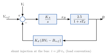
The SVC voltage regulator: integrator with reactive droop; the susceptance \(B\) is injected as a shunt at the bus.#
- class hermess.devices.svc.SVC[source]
- Static var compensator: a voltage-regulated shunt susceptance
(Gibbard and Vowles 2014, Appendix I.2.3, Fig. 22, converted from the SVC Mvar base to the system base).
Selected in a system file by its class name in the first column, e.g.
SVC, idx = "ASVC_2", bus = "205", KA = 500, q = -68.3.Model. Integrator voltage regulator with a droop on the deviation of \(Q/V_t = B V_t\) from its initial operating point, a thyristor-control lag, and the shunt current injection (load convention):
\[\begin{split}e &= V_{ref} - V_t - K_d \left( B V_t - B_{ref} \right) \\ \dot{x}_B &= K_A \, e \\ T_d \, \dot{B} &= 2.5 \, x_B - B \\ \bar{i} &= \mathrm{j} B \bar{v}_n \quad\Longleftrightarrow\quad i_{re} = -B v_{n,im}, \;\; i_{im} = B v_{n,re}\end{split}\]with \(V_t = |\bar{v}_n|\) the bus-voltage magnitude and \(B\) the susceptance in p.u. on the system base (\(B > 0\) injects \(Q = B V_t^2\)). The factor 2.5 is the fixed gain of the published thyristor block. With
incl_limthe limiter loop enforces \(B^{min} \le B \le B^{max}\).Initialization is sequential (closed form): the initial reactive output
q[Mvar] is a device input (the loadflow result at the SVC bus, e.g. Table 9 of the SEA benchmark), from which\[B_0 = \frac{q / S_b}{V_0^2}, \qquad x_{B,0} = \frac{B_0}{2.5}, \qquad V_{ref} = V_0, \qquad B_{ref} = B_0 V_0 .\]SVC buses typically also carry loads, and a joint Newton solve would attribute the whole bus current to this device; the SVC therefore removes its share of the bus current from the initialization residual, so co-located devices calibrate themselves from the remaining injection (SVC entries must precede those devices in the system file). Consistency with the power flow is verified by the zero-residual initialization check.
Symbols.
Code
Symbol
Meaning
Default
KA\(K_A\)
voltage-regulator integrator gain [p.u. B / s / p.u. V]
500
Kd\(K_d\)
Q/V droop gain [p.u. V / p.u. Q]
0.01
Td\(T_d\)
thyristor-control lag time constant [s]
0.005
B_min/B_max\(B^{min,max}\)
susceptance limits, system base (with
incl_lim)-10 / 10
q\(q\)
initial reactive output from the loadflow [Mvar]
0
xB\(x_B\)
regulator integrator state [p.u.]
B\(B\)
shunt susceptance (state) [p.u.]
Vref\(V_{ref}\)
voltage reference (set to \(V_0\) by the initialization)
Bref\(B_{ref}\)
droop anchor (set to \(B_0 V_0\) by the initialization)
Sn\(S_n\)
rated power (inherited device rating) [MVA]
100
Vn\(V_n\)
rated voltage (inherited device rating) [kV]
220
fn\(f_n\)
nominal frequency (inherited device rating) [Hz]
50
u\(u\)
connection status (inherited device flag)
True